1. What is the mean by “Premium”?
The PCB Service can meet >95% customer’s requirements, but for some customers, especially makers who have experience on hardware developing and projects that need many special requirements. They need more reliable& advanced PCB service, such as multiple layers more than 4, blind holes, FPC. That’s why we PCBWave provides this “Premium PCB Service”.
2. What’s the main upgrading compared to the common PCB services?
This “Premium PCB” service is based on “One-by-One Quotation”, so we would be able to meet your personal requirements . Compared to the common PCB service, the main upgrading is:
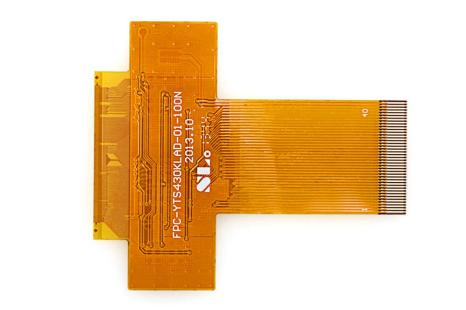
Support More Kinds Of PCB: FPC/ Rigid-flex PCB are avaible now at PCBWave ;
More Professional PCB Specifications: PCB Multilayers 1~28; Blind holes; Copper thickness up to 3oz; Thinner/Thicker PCB thickness 0.2mm~6mm;
More Reliable Quality: Sharper silk screen; 100% E-test + 100% visual check.
More color for PCB(Include Matte Black, Matte green and purple); Minimum PCB track /Space up to 3 mil.
For FR-4 PCB, please refer to the detail specifications& comparision with common PCB service:
Multilayer PCB
The Multilayer PCB can be used on electric services, such as cell phone transmission, cell phone repeaters, computer motherboard, data storage and GPS technology. In order to reduce signal loss, use a multi-layer shield signal, such as the base station, the communication class. Besides, it also can be used on medical equipment: X-ray equipment, heart monitors and so on.
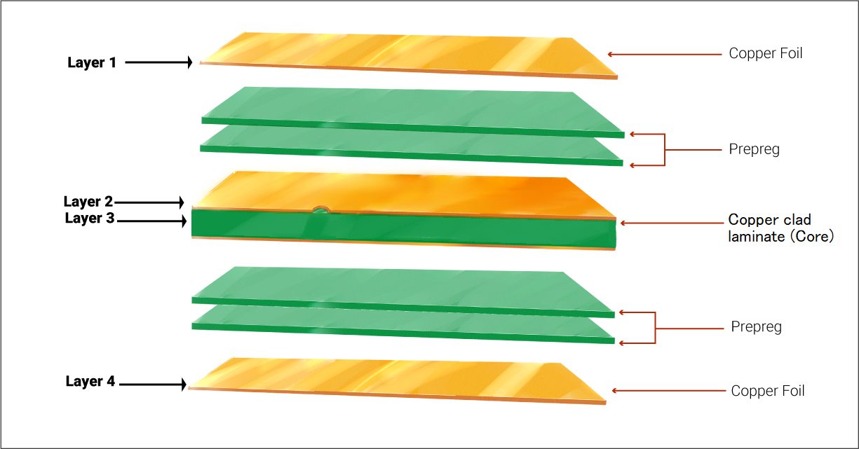
Please refer to the below details and specifications:
|
Multilayer PCB |
|
|
Parameters |
Capability |
|
MULTI LAYERS |
1-22 |
|
Finished BOARD THICKNESS |
0.2mm-6.0mm |
|
FINISHED COPPER THICKNESS |
0.5oz-12oz |
|
MIN TRACE WIDTH |
0.075mm |
|
MIN BLIND VIA |
0.1mm |
|
MIN V-GROOVE PCB THICKNESS |
0.6mm |
|
MINIMUM BGA PAD/SPACE |
0.2mm/0.1mm |
|
PLUG HOLE SIZE |
0.2-0.4mm |
|
Material |
FR4, Aluminum, Rogers, Polyimide |
|
SURFACE FINISH |
HASL, HASL (Lead Free), ENIG, OSP |
|
WARP& TWIST |
≤0.75% |
|
N/C ROUTING TOLERANCE |
±0.1mm |
PCBWave is devoted to provide Aluminum substrate, if you are looking for an Aluminum substrate, our engineer can meet your requirement. Aluminum substrate is a kind of copper-clad circuit board based on metal substrate, with good thermal conductivity. A thin layer of thermally conductive but electrically insulating dielectric is laminated between a metal base and a copper foil. The copper foil is etched into the desired circuit pattern and the metal base draws heat away from this circuit through the thin dielectric.
It can be used on the following areas:
- Audio equipment: input, output amplifier, balanced amplifier, audio amplifier, preamplifier, power amplifier, etc.
- Power equipment, switching regulator, DC/AC converter, SW regulator, etc.
- Communication electronic equipment: high frequency increaser, filtering appliances, transmitting circuit.
- Office automation equipment, motor drives, etc.
- Automobile electronic regulator, ignition, power controller, etc.
- Computer: CPU, a diskette drive, power supply units, etc.
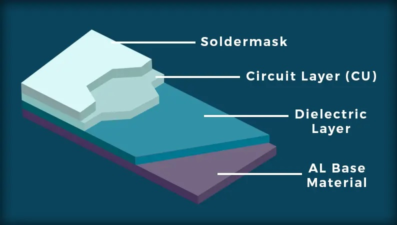
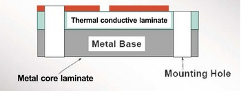
This structure need more technology and experience on laminating of two layers together with metal core.
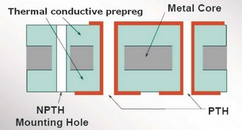
|
Aluminum PCB(MC PCB, AL substrate) |
|
|
Parameters |
Capability |
|
MULTI LAYERS |
1-2-4 |
|
Finished BOARD THICKNESS |
1.0mm-2.0mm |
|
MIN TRACE/SPACING |
≥5mil |
|
MIN HOLE |
≥0.5mm |
|
SURFACE FINISH |
HASL, ENIG, OSP |
|
FINISHED COPPER |
1oz, 2oz |
|
Solder mask color |
Green, Blue, Yellow, Red, Black, White |
Here are the general benefits of our Flex PCB service
1. Excellent Flexibility: Stable and repeating flexibility is helpful for 3-D electronic products assembly.
2. Lower Toughness: Lower toughness is benefit for standing more thermal stress and reducing the joint cracking risk.
3. Thin dielectric: Thin dielectric could have better flexibility and better heat transfer, those will be benefit for structure design and thermal management.
4. Great high temperature performance: PI material could be operated under high temperature environment then can fit for high temperature applications.
5. Good manufacturability: Some flexible material can use laser or chemical etch create pads or window then could be used in double access applications.
6. Multi-plane connection and size shrinking: Flexible boards could be bended and binding with rigid-flex technology then can reduce connector and terminator using that can reduce weight.
7. High space utilization: Flexible boards can replace many connecting parts and join multi plane boards then by these strength can saving space and make design easier.
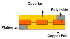
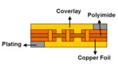
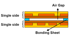
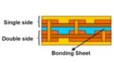
Here are the basic structure of Flex PCB
|
Single Side Double Access |
Double Side |
Single side plus Single Side |
Multi-layers |
 |
 |
 |
 |
Here are some regular FPC in the application
|
FPC for Antenna |
FPC for Notebook Camera |
FPC for Winding Displacement |
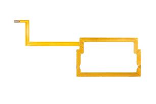 |
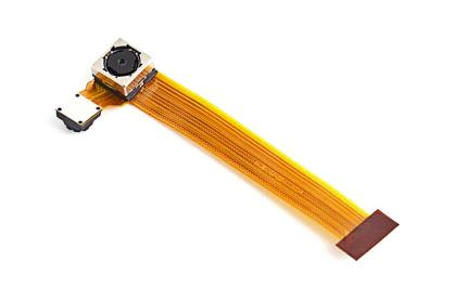 |
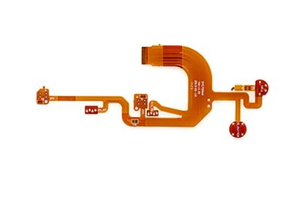 |
|
FPC for Button |
FPC for Monitor |
FPC for LED Module |
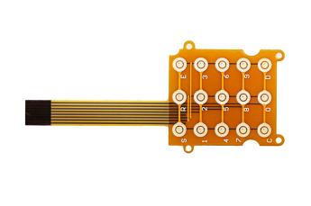 |
 |
 |
Please refer to the below details and specifications:

3. How to begin my “Premium PCB” Service?
- 1. Download the Premium PCB Specifications and input your PCB demands, if you do not know how to selector for some of the parameter, just leave it as it is.
- 2. Sent this file and your gerber files to service@pcbwave.com. For the gerber files, please refer to here.
- 3. We PCBWave will quote it for you in 1~3 working days. If you think it OK, after your paying, we will make your PCB into production. The fabrication time will be 3~12 days(excluding Chinese Festival).
- 4. Note that the 300$ free shipping policy do not apply to the Premium PCB service.


